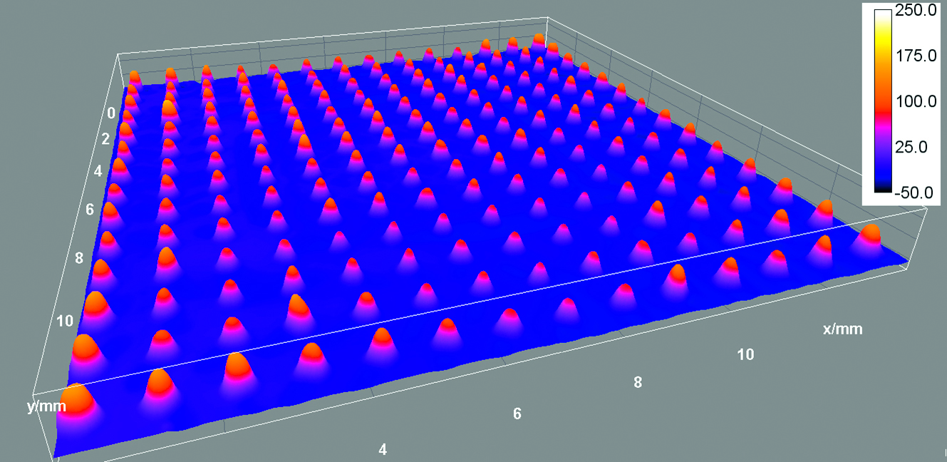
The Fraunhofer Institute for Physical Measurement Techniques IPM, Freiburg, uses, among others, the method of digital multi-wave holography for fast and highly accurate measurements of surfaces, with which measurements in the sub-micrometer range are possible with very short measuring times. Whereas previous applications were mainly limited to small, matchbox-sized workpieces, a new development is now available that can also be used to measure components with surfaces up to 190 mm x 150 mm in size. One example of this is the quality control of high-current circuit boards for use in wind turbines. With the new holography system, these can be inspected over their entire surface for micrometer-sized defects with just one exposure and a measurement time of less than one second.
During a measurement, the test specimen to be measured is irradiated with laser light, which partially scatters the light back to the sensor. This backscattered light is usually collected with a lens and directed onto a camera. There it is superimposed with unaffected laser light. The resulting interference images of the two laser beams carry information about the shape of the object. This can be obtained from the recorded interference images by numerical calculations. If the measurement is repeated with several slightly different laser wavelengths, measurement accuracy and range can be increased. By selecting the laser wavelengths and the optical setup, the method can be adapted to different application areas in an application-specific manner.
In contrast to classical interferometry or holography with only one laser wavelength, multi-wavelength holography can be used to measure optically rough surfaces. The speckle noise generated on rough surfaces, which normally makes quantitative phase evaluations for topography determination impossible, is eliminated by numerical reconstruction at different wavelengths. This produces a phase map at the beat frequency of the individual wavelengths, which contains the information about the topography of the illuminated object and can be evaluated quantitatively.
Typical applications of the method are wherever imaging 3D inspection must be fast (second cycle or faster) and accurate (in the micrometer range). Areas of application include the detection of defects (pores, delaminations, etc.) or the inspection of dimensional compliance of workpieces (test specimens slightly distorted by a few µm over a length of 200 mm). Thus, electrical contacts (bumps) with a height of 50 µm can be precisely inspected and the smallest deviations that would impair functionality can be localized.
